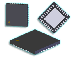
Figure 1: QFN Component Package Pictures
The Quad Flat No-lead (QFN) package is a CSP (plastic encapsulated package) with a copper lead frame substrate. The QFN is a leadless package where electrical contact to the PCB is made by soldering the leads on the bottom surface of the package to the PCB, instead of the conventional formed perimeter gull wing leads. The design of the QFN package has enhanced electrical performance that enables the standard 2 GHz frequency to be increased up to 10 GHz with some design considerations.
The QFN leads are coated with a finish that provides environmental protection and maintains solderability. See Figure 2 for a cross-section internal view of the QFN package construction.

Figure 2 - QFN Construction
The symmetric termination leads can be either rounded ends or rectangle ends. See Figure 3 for the 2 different lead styles.

Figure 3 - QFN Lead Shapes
The QFN uses the “Flat No-lead Edge” component lead style. See Figure 4 for a side view of the component lead. The component lead terminals are embedded in the plastic body and sticks out 0.05 mm on the bottom and wraps up the component body side by 0.2 mm.

Figure 4 - Flat No-lead Edge Terminal Type
There are 2 types of QFN component package styles, Standard & Flanged Type. The Standard package is commonly known as the “Saw Cut” package and the Flanged Type is known as “Molded Body”. See Figure 5 for the 2 types of component package styles.

Figure 5 - QFN Component Package Styles
The Thermal Tab shape can have a chamfered corner closest to the location of Pin 1. The “Land Size” is identical to the maximum tolerance of the thermal tab size. The solder mask size is 1:1 scale of the land size. The thermal tab can also have corner radius on the other corners. See Figure 6 for an example of a thermal tab with chamfered and rounded corners.
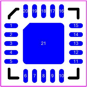
Figure 6 - Thermal Pad with Chamfer & Rounded Corners
The Thermal Pad Paste Mask size needs to be between 40% and 60% of the land size and is broken up into a checkerboard pattern. The IPC LP Calculator is set to 40% paste mask reduction by default, but the reduction percentage is user definable. The checkerboard pattern does not start until the thermal pad size exceeds 4.5 mm because the minimum paste mask aperture opening for thermal pad paste mask is about 1 mm square. See Figure 6 for examples of thermal tab paste mask with a 40% reduction. The picture of the left has a thermal pad size of 4 mm and a single paste mask of 2.5 mm. The picture on the right has a thermal pad size of 4.5 mm and a matrix of 4 squares of paste mask of 1.4 mm.

Figure 7 - Thermal Pad Paste Mask with 40% Reduction
If there was no reduction of paste mask, the physical component would float on top of 0.15 mm (the thickness of the paste mask stencil) of solder. During the reflow process users have observed that the liquidus solder lifts the device and creates a pivot point near the center of the Die Attach Pad (DAP). As the solder cools the device tends to tilt toward one side, often creating shorts in one area and opens in another. By reducing the paste mask stencil to 40% of the land size, the component will settle down evenly to allow for an adequate solder joints on the end termination leads. See Figure 8 for an example of excessive solder and reduced solder on the Die Attach Pad.

Figure 8 - Excessive Thermal Pad Paste Mask
The primary purpose of the thermal tab is to conduct heat away from the die during operation. The best way to achieve this goal is to add stitch vias attached to the GND plane. The via hole size recommendation is 0.25 mm and should be plated, plugged and surface finished to prevent liquidus solder from entering the holes. By no means attempt to Tent the vias with dry film solder mask because this will reduce the solder volume area on the pad. The via padstack is 0.5 mm pad, 0.7 mm plane clearance, 0.25 mm hole and no thermal relief. Placing the vias on a 1 mm grid allows for two 0.1 mm trace/space routing technology on all inner layers and opposite side. In order to achieve the 1 mm via snap grid, the QFN must be placed on a 0.5 mm placement grid. See Figure 9 for an example of a via matrix in a thermal pad.

Figure 9 - QFN Thermal Pad Via Stitching
Some QFN packages come in a variety of lead sizes and multiple thermal tabs. See Figures 10 – 12 for some unique QFN variations.
Figure 10 has multiple lead lengths and “Deleted Pins”.

Figure 10 - QFN with Different Lead Lengths
Figure 11 QFN has multiple thermal tabs and “Hidden Pins”. Some QFN packages have 3 – 5 thermal tabs with various shapes and sizes.

Figure 11 - QFN with Multiple Thermal Tabs & Deleted Pins
Figure 12 QFN has deleted pins and Pin 1 is lower left corner and pin order is Counterclockwise instead of the traditional Clockwise pin order.

Figure 12 - QFN with Deleted Pins & Pin 1 in Lower Left w-Counterclockwise pin order numbering

Figure 13 - QFN Land Pattern Details
The via fanout for the QFN component family is really easy for all pin pitches that are on even 0.1 mm increments. These are 0.8 mm, 0.5 mm and 0.4 mm pin pitch. All SMT components with a 0.65 mm pin pitch are not 100% compatible with the 0.05 mm universal grid system. It would be superior if the component manufacturer’s never created any pin pitch in 0.05 mm increments. It would be much better for the PCB designer if all pin pitches were in 0.1 mm increments. In this case, 0.65 mm pin pitch would be superior if it was 0.6 mm. Let’s take a look at some of the via fanout solutions to optimize routing channels. All of the routing solutions use the identical via size (0.5 mm pad, 0.7 mm anti-pad and 0.25 mm hole) and trace/space (0.1 mm) technology that is located in Figure 9.
Figure 14 is a 0.8 mm QFN sample via fanout and routing channel solution. This routing solution provides for 1 trace between vias. The red traces are the opposite side and the green traces are the inner layer. The yellow annular ring on the via is the plane clearance. A 0.1 mm grid was used for the via fanout and trace snap grid.

Figure 14 - 0.8 mm Pitch QFN Via Fanout & Routing Solution
Figure 15 is a 0.65 mm QFN via fanout and routing channel solution. The 0.65 mm pitch fanout must use a 0.05 mm grid and 3 traces between vias. When there is an even number of pins on each side, you have to use a 0.025 mm grid system because the components are always placed on a 0.1 mm grid system and from the center of the 0.65 mm QFN to the center of the pad is 0.65 divided by 2 = 0.325 mm. This is why 0.65 mm pitch components are not optimized for the universal 0.05mm grid system.

Figure 15 - 0.65 mm Pitch QFN Via Fanout & Routing Solution
Figure 16 is a 0.5 mm QFN via fanout and routing channel solution. This routing solution provides for 2 traces between vias. A 0.1 mm grid was used for the via fanout and trace snap grid.

Figure 16 - 0.5 mm Pitch QFN Via Fanout & Routing Solution
Figure 17 is a 0.4 mm QFN via fanout and routing channel solution. This routing solution provides for 1 trace between vias. A 0.1 mm grid was used for the via fanout and trace snap grid.

Figure 17 - 0.4 mm Pitch QFN Via Fanout & Routing Solution