Periphery Solder Joint Goals
When it comes to solder joint goals, we are familiar with the terms Toe, Heel and Side solder joint fillets, but IPC introduced the Periphery solder joint in the latest release of the IPC-7351B. Due to the indoctrination of several new component families like Dual Flat No-lead (DFN), Land Grid Array (LGA), Pull-back Quad Flat No-lead (PQFN), Pull-back Small Outline No-lead (PSON) and Column Grid Array (CGA), IPC created the Periphery solder joint goal to accommodate these “Bottom only terminal” lead forms as seen in Figure 1.

Figure 1 - Components with Bottom Only Terminal Leads
The flat leads of these component families are very compatible with lead-free solder, due to the fact that some lead-free solder alloys have low-flow wetting properties. The flat lead with a Periphery land area also improves assembly accuracy as the components have minimal “wander” movement during the reflow process. This is unlike the typical chip resistor & capacitor has a wrap-around component lead. Great caution must be taken into consideration because the J-STD-001D assembly standard allows for chip component overhang of up to 50% of the component width for Class 1 and Class 2 and 25% for Class 3 (the “A” dimension) as seen in Figure 2.
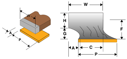
Figure 2 - Acceptable Wrap-around Lead Solder Joint
The new DFN component family has 2, 3 and 4 lead package styles and the body sizes range from 16 mm to 1 mm in size. The 2-pin DFN package is intended to replace wrap-around leaded chip resistors, diodes and capacitors. The component terminal leads for pin 1 and 2 can be different sizes. The DFN component package data is derived from the JEDEC MO-236A standard. The 3-pin DFN package is intended to replace gull wing leaded SOT23 and DPAK transistors and voltage regulators. The 4-pin DFN package is intended to replace a variety of different component families including oscillators, bridge rectifiers, LED’s, sensors, etc. The Periphery solder joint goals as seen in Table 1 are used for the DFN, PSON and PQFN component families.

Table 1 - DFN, PSON and PQFN Solder Joint Goals
The LGA component family usage is rapidly growing. The LGA component lead style can be a bump which is typically a round shape. The LGA component lead style can also be flat which can be round, square or irregular shape. The pin assignments typically follow the same JEDEC convention as BGA’s. The LGA component package data is derived from the JEDEC MO-270B standard. See Figure 3 for the LGA lead styles.
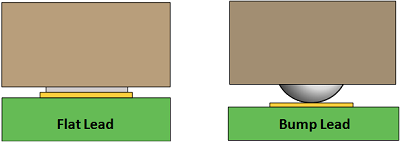
Figure 3 - LGA Lead Styles
See Figure 4 for the LGA lead shapes.
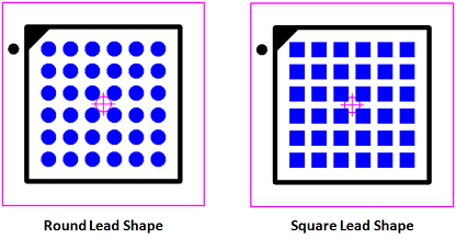
Figure 4 - LGA Lead Shapes
The LGA land pattern only has one tier environment similar to the BGA however; the LGA land size is 1:1 scale of the lead size. See Table 2 for the LGA solder joint goals.
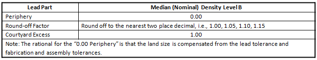
Table 2 - LGA Solder Joint Goals
Multi-row & column LGA’s will require via-in-pad routing solutions for the inner rows of contacts because there is no room for the traditional “dog bone” via fanout. Figure 5 represents a 1.0 mm pitch LGA with 0.7 X 0.7 mm square lands with a flat lead. You can place 0.5 mm pad & 0.25 mm hole vias in the center of the lands and be able to route two 0.1 mm traces between the vias.

Figure 5 - LGA Via Fanout
Unlike Pin Grid Arrays (PGA) that have been common to microprocessors, LGA’s do not utilize any pins but rather an array of bare gold plated copper pads that permit a direct electrical connection between the component substrate and the PCB. Compared to the PGA component family, LGA pad density can be significantly higher due to tighter spacing that is not hindered by the need to attach pins to the substrate.
Linear Technology is the world’s leading producer of LGA component packages. Linear uses unpopulated component leads in many of its component packages as seen in Figure 6.
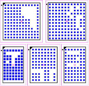
Figure 6 - Linear LGA Packages with Unpopulated Leads
The BGA land is considered the first “periphery” land introduced to the electronics industry. However, the collapsing BGA ball is the only land calculation that creates a smaller land than the component lead. Non-collapsing BGA balls require a larger land size than the ball size. Via-in Pad in a flat lead LGA produces better solder joint results than BGA technology because there are no “Voids” in the flat LGA component lead after reflow. Figure 7 is a BGA ball cross-section that illustrates trapped air hole using via-in-pad BGA void issues.

Figure 7 - BGA Void
However, voids created by trapped air in blind or through-hole vias can be eliminated by plugging or filling the hole prior to the land plating process. Figure 8 illustrates various types of vias that contribute to trapped air and that causes voids in BGA balls.

Figure 8 - BGA Voids From Trapped Air
The Pull-Back Small Outline No-lead package (PSON) is a rectangular semiconductor package with metal terminals along two sides of the bottom of the package. The Pull-back leads are typically 0.1 mm to 0.2 mm away from the component body edge. The body of the component is generally molded plastic and the plastic mold compound is present on all 4 sides of the terminal lead contact. The SON and PSON component families are intended to replace the leaded SOIC and takes up about 50% less PC board area footprint. The PSON is considered a leadless package design with a bottom paddle to conduct heat away from the package used stitch vias that attach to the GND plane.
The Pull-back component lead terminal shown in Figure 9 represents the Pull-back Small Outline No-lead (PSON) and Pull-back Quad Flat No-lead (PQFN) which have two different lead shapes, D-shape and rectangular. These illustrations are 0.8 mm pitch 5 mm X 5 mm body outline.
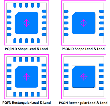
Figure 9 - PSON & PQFN Lead Shapes
Note: the latest LP Wizard and LP Calculator 10.3.1 release introduces the D-shape land calculation and CAD export to tools that support D-shape lands.
See Table 1 for the IPC-7351B 3-Tier land pattern environments for PSON and PQFN component lead form with the Periphery solder joint goals.
Ceramic and Plastic Column Grid Arrays (CGA) solder column contacts are used for larger ceramic-based packages (32.0 mm to 45.0 mm). The package resembles the earlier plated through-hole pin-grid-array but with closer contact pin pitch. The column contact diameter is typically 0.5 mm for 1.0 mm pin pitch and 1.2 mm to 2.0 mm lead length. The columns are attached to the package either by eutectic (Pb37Sn63) solder or they are cast in place using 90% Pb and 10% Sn. Via-in-pad technology is popular with the 1.0 mm pitch CGA component family due to the lack of room for a typical bog-bone via fanout.
The longer columns typically increase solder joint reliability by absorbing the stresses created by the CTE mismatch between the ceramic package and the PC board. On the other-hand, longer columns may reduce electrical performance and will increase the overall package profile on the PCB. Also, the columns are not as rugged as a BGA solder joint and are susceptible to handling damage.
The Column Grid Array was grouped with the LGA component family solder joint goals in the IPC-7351B at 1:1 scale lead to land size, but the CGA solder goals were recently been updated so that the land size is 0.1 mm larger than the maximum lead diameter. Figure 10 illustrates the CGA solder joint goal with a periphery land to form a solder fillet and Table 3 has the solder joint goal data.
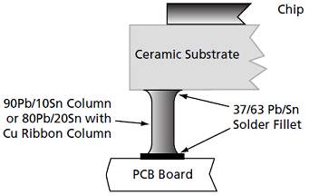
Figure 10 - CGA Solder Joint
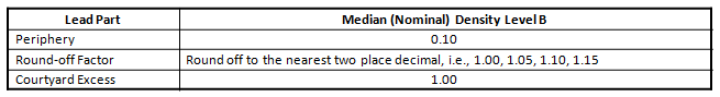
Table 3 - CGA Solder Joint Goals
The DFN, PSON, PQFN, LGA, CGA and BGA have a different concept for developing a land pattern. Effectively, there are no toe, side or heel fillets; rather the land periphery is similar about the entire termination. Whether the component terminal shape is round, square, rectangle or D-shape, once the tolerance is assigned it applies to the periphery of the lands for that particular part. Thus the term “Periphery” is used to signify that the principles occur all around the component package termination contact.
Did you know that the LP Wizard fully supports all the component families listed in this article? You can download the free 10-day trial license for the newly released LP Wizard 10.3.1 that now produces D-shape land style for PQFN and PSON component families here – http://www.mentor.com/go/lpwizard
After the 10-day trial license ends, there is no need to uninstall the program as the LP Wizard will run in “Demo Mode” (without a license) as an IPC-7351B LP Calculator.