PCB Breakaway Panels
As PCB part placements get denser, it’s necessary to add breakaway panels that add additional board material (edge rails) to accommodate the assembly process. Two parallel edges are required for a PCB to be processed in the SMT line. This is to prevent skewing through the conveyor system. Also, all odd shaped PCB’s must have edge rails incorporated to meet this requirement. Custom reflow fixtures will be made, at an additional cost to you, if this requirement is not met. The breakaway tabs remain intact all the way through the assembly process and are removed at the final stage.
V-Grove Score and Tab Routing are two common methods used for creating breakaway tabs. Tab Routing uses perforated breakaway tabs (sometimes referred to as “Mouse Bites”). The breakaway tab closest to the PCB corner should be located between 10 mm and 12 mm from the edge to reduce sagging during reflow or wave soldering. It is also preferred to have at least one tab per side. If the PCB placement is too dense for a Tooling Hole, then it should be placed on the breakaway tab. See Figure 1 for the optimized breakaway tab solution.
Note: all dimensions in this paper are in millimeter units.

Figure 1 - Example of Breakaway Panel
One important aspect is to have a clean edge after the breakaway tab is removed. Slight inset of perforation is preferred because it provides an edge which requires little to no additional labor to clean up. Figure 2 illustrates the perforation location preferences.
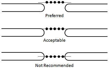
Figure 2 - Breakaway Perforation Locations
The spacing between breakaway tabs can range from 60 mm to 90 mm, but I recommend 77 mm from center to center as shown in Figure 3. Try not to exceed 100 mm between tabs and try to evenly space them apart.
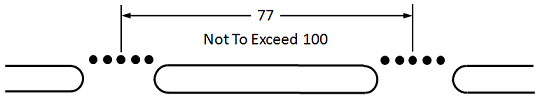
Figure 3 - Breakaway Tab Spacing
The plane pull-back should be at least 1 mm from all slots and perforation holes. All trace routing needs to be over a plane for clean return path so keep all routing 1 mm from all slots and perforation holes. Keep components 2 mm – 3mm away from the routed slots. These rules help prevent components or trace damage during the de-paneling process. See Figure 4 to define the keep-out areas in the PCB layout.

Figure 4 - Plane & Component Spacing
Tab routing is more precise than V-groove scoring and edge surfaces are smooth. The breakaway tab points require consideration for additional smoothing if necessary to comply with the fabrication drawing note regarding smooth edges. The dilled perforation provides a low stress break point on the tab and if the hole pattern is recessed within the printed board edge, secondary sanding or grinding can be avoided.
It is not recommended to substitute perforation holes with a V-groove score as it does not provide a durable tab that will withstand handling. V-groove scoring can however be used in place of routing, but requires board edge grinding to smooth the surface. The V-groove feature is generally provided on both sides of the PCB and only in a straight line. A V-Groove depth that will provide a sturdy work-piece and still separate with light to moderate pressure after assembly is an important element in manufacturing. Many PCB fabrication shops recommend a V-grove depth that is 1/3 of the PCB thickness from both sides using Computer Numerical Control (CNC) equipment. The alignment or positional accuracy of the two grooves is critical for clean separation and minimizes post separation board edge smoothing. According to IPC-2222 Section 5.3.1, the alignment tolerance for the V-groove is ±80 µm. Figure 5 illustrates the 90° scoring option. It is important that all conductors be routed within a minimum distance of 1 mm from the top of the scoring edge to prevent damage during de-paneling. The inner layer planes should be pulled back 1 mm from the V-groove. The PCB designer should collaborate with the PCB fabrication shop on the V-groove angle option that they use.
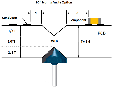
Figure 5 - 90 Degree V-Groove Scoring
Figure 6 illustrates the 30° scoring option and uses the same rules.

Figure 6 - 30 Degree V-Groove Scoring
It is important to note that the 1/3 depth rule only applies to “Breakaway Panels”. V-Groove scoring inner web material can range from 0.15 mm to 0.4 mm for panel separation depending on the length of the score. If the score length is less than 25 mm, it can have a web thickness of 0.15 mm and scores that are 100 mm long can have a web thickness of 0.25 mm and scores that are longer than 100 mm can have a web thickness of 0.4 mm. These values are just guidelines and should be discussed with your assembly shop to confirm the web thickness for your printed circuit board design.